


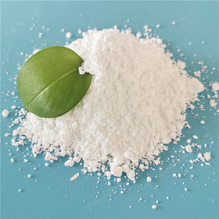
The core technical highlights of this product include customizable nanoparticle sizes ranging from 10-15nm, a stable colloidal dispersion system and ultra-low heavy metal content that meets the semiconductor material purity requirements. It corrosion risks to precision polishing equipment, and forms a uniform, scratch-free polishing layer. It solves the pain points of traditional polishing agents such as high residual impurities, low surface flatness, and high equipment wear, significantly reducing post-processing workload and production costs.
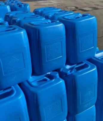
The product has a SiO2 content of 30.0±0.5%, with a particle size of 12±2nm, viscosity of 4.2 mPa·s, pH value of 9.5, and conductivity of 8 μS/cm. Its density is 1.21 Grams/Cubic Centimeter, and it is packaged in 25-kilogram food-grade plastic cartons. It has a freeze-thaw stability of 5 cycles without performance degradation, and can be stored stably at temperatures ranging from 5℃ to 30℃. It complies with SEMI S2 safety standards and has passed multiple third-party purity tests to ensure consistent quality across batches.
This product is primarily applied in semiconductor wafer chemical mechanical polishing (CMP), LED chip substrate polishing, photovoltaic silicon wafer pretreatment, precision ceramic component polishing, and semiconductor packaging material modification. It is suitable for the production of 12-inch and 8-inch silicon wafers, high-brightness LED chips, and precision optical components, providing excellent surface flatness and dimensional accuracy for high-end electronic manufacturing industries.


 Post RFQ


 Chat
Chat


 ALL CATEGORIES