


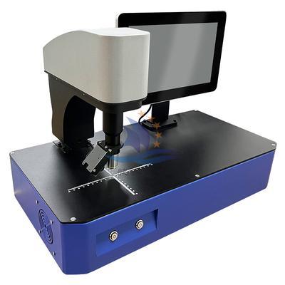
It adopts 6 sets of 12MP high-resolution industrial cameras, matched with coaxial oblique light source and dark field light source, which can detect nano-scale scratches, impurities and protrusions on the wafer surface. Its built-in deep learning-based semiconductor defect recognition model covers more than 99.9% of common semiconductor defect types. It supports full-size inspection of 300mm diameter wafers, and can upload inspection data to the semiconductor production MES system in real time. It supports precise positioning and classification of wafer defects, and meets the SEMI S2 semiconductor safety standards to ensure that the inspection process complies with industry specifications.
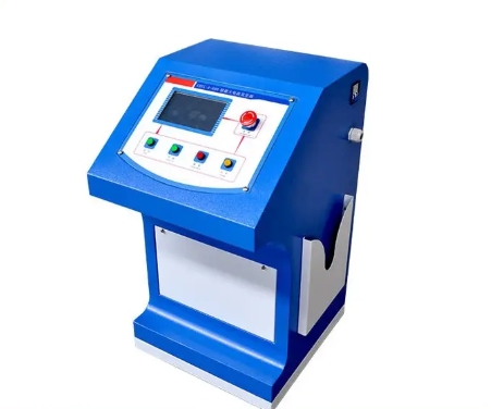
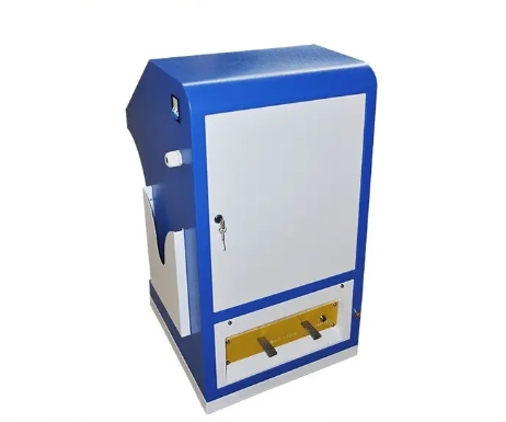
The maximum detection area is wafers with a diameter of 300mm, and the minimum detectable surface defect is 0.001mm. The camera resolution is 12 million pixels, and the detection speed is 150cm² per second. The power supply is AC220V 50/60Hz with a power consumption of 1.8kW. The overall dimensions are 1600*1400*1700mm, and the equipment weight is 950kg. It supports wafer thickness of 0.05-0.8mm, and is equipped with a high-precision motion platform with a positioning accuracy of 0.0005mm. It supports automatic loading and unloading docked with semiconductor packaging production lines, and has passed CE, ISO9001 and SEMI S2 certifications.
It is mainly applicable to semiconductor wafer manufacturing factories, IC packaging and testing factories, micro LED manufacturing enterprises and other high-end manufacturing enterprises. As the inspection equipment for wafer surface defects, chip pin defects and micro LED light point defects, it meets the high-precision quality inspection requirements of high-end semiconductor manufacturing, helping enterprises reduce the outflow of defective products and improve the reliability and yield of semiconductor products, complying with global semiconductor industry quality control standards.


 Post RFQ


 Chat
Chat


 ALL CATEGORIES