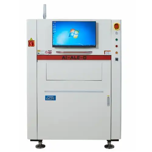
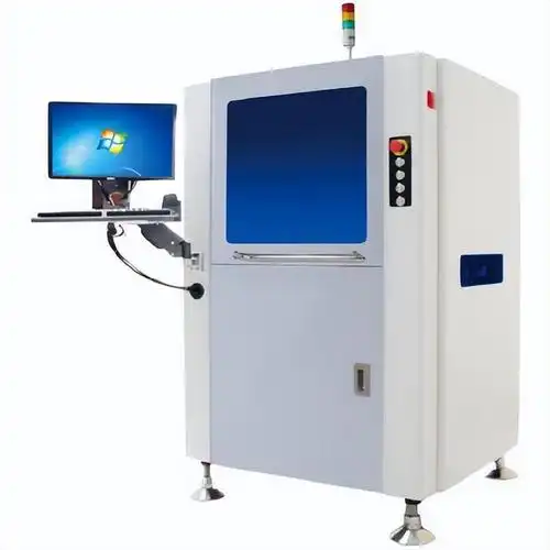


It adopts 4 sets of 5MP industrial cameras and combined light source to eliminate the reflection problem of PCB surface, and its built-in AI algorithm library covers more than 99% of common PCB defects. The equipment can be docked with the existing MES system to realize real-time uploading of inspection data and automatic generation of defect reports. It supports remote debugging and fault early warning, which reduces the operation and maintenance costs of the production line. Compared with manual inspection, it can improve the inspection efficiency by more than 3 times, and effectively solve the quality inspection bottleneck in large-scale PCB production.
The maximum detection area is 610mm*510mm, and the minimum detectable solder joint defect is 0.03mm. The camera resolution is 5 million pixels, and the detection speed is 1200cm² per second. The power supply is AC220V 50/60Hz with a power consumption of 1.5kW. The overall dimensions are 1800*1200*1600mm, and the equipment weight is 850kg. It supports PCB thickness of 0.1-3.2mm, and is equipped with AI defect recognition model that supports custom defect training. The communication interfaces include Ethernet, USB3.0 and RS485, and it has passed CE, FCC and ISO9001 certifications.
It is mainly applicable to SMT patch processing plants, PCB rigid board/flexible board manufacturing factories, consumer electronics assembly plants and other enterprises. As the online quality inspection equipment at the back end of the production line, it replaces manual visual inspection, and is suitable for defect detection of products such as mobile phone PCBs, computer motherboards and automotive electronic PCBs. It can be docked with the existing production MES system to realize the traceability of the whole process of quality inspection data, and improve the production yield by more than 5%.


 Post RFQ


 Chat
Chat


 ALL CATEGORIES