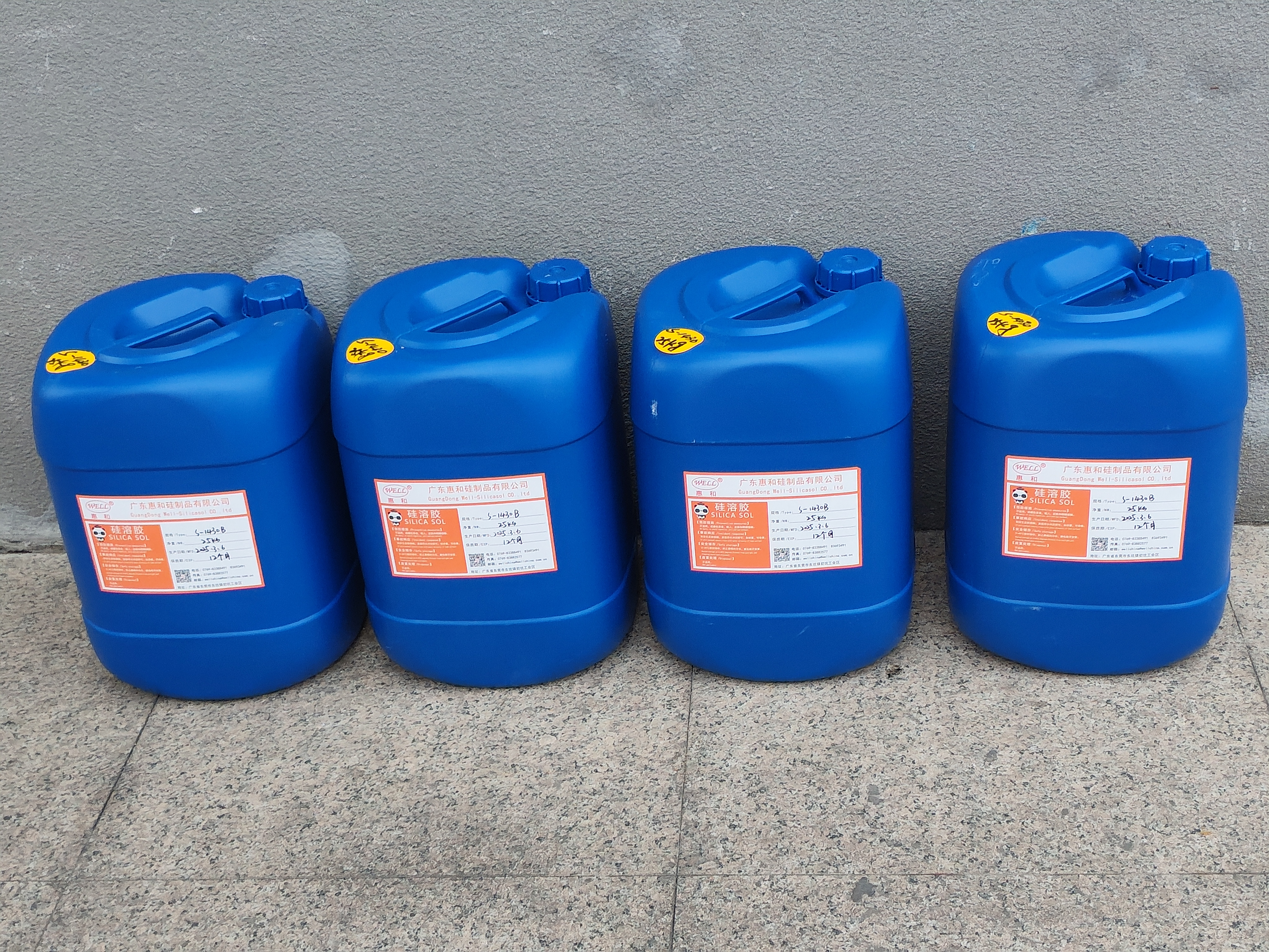





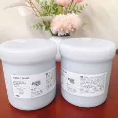
This silica sol has core competitive advantages including ultra-high purity, adjustable particle size, high polishing efficiency, and minimal substrate damage. It complies with SEMI international semiconductor industry standards, with total metal impurity content of ≤10 ppb, which will not cause pollution to semiconductor manufacturing equipment or affect the performance of electronic components. The uniform particle size distribution ensures stable polishing effect, reducing the surface roughness of the base material to the nanometer level, and improving the yield of electronic component manufacturing.
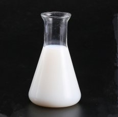
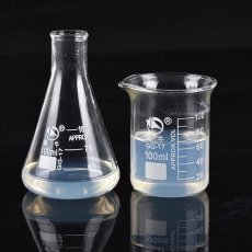
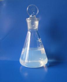
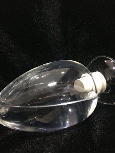
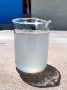
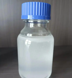
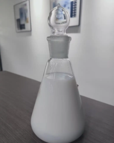
Key technical parameters include SiO2 content of 30±0.3 wt%, adjustable particle size ranging from 5 to 15 nm, total metal impurity content of ≤10 ppb in line with SEMI standards, viscosity of 4-12 mPa·s, pH value between 9.5 and 11.0, residual ammonia content of ≤50 ppm, shelf life of 24 months, appearance as colorless transparent liquid, bulk density of 1.20 g/cm³, and no flash point as an aqueous solution. It can be customized according to the specific polishing needs of customers, including adjusting particle size and concentration.
This product is widely used in chemical mechanical polishing (CMP) of semiconductor wafers, polishing of LED sapphire substrates, polishing of touch screen glass, surface treatment of electronic packaging materials and other electronic manufacturing fields. It is mainly supplied to semiconductor wafer manufacturing plants, LED manufacturing enterprises, touch screen processing enterprises and other high-tech electronic manufacturing industries, helping them improve product quality and production yield.










 Post RFQ


 Chat
Chat


 ALL CATEGORIES