Automated Wafer Level Profile Metrology System
next
prev
Video
1/2

Automated Wafer Level Profile Metrology System

Price
MOQ
$27999
1 Pieces
Product Details
Measuring Range:
200mm Wafer / 300mm Wafer
Measurement Accuracy:
±0.05μm
Scanning Speed:
20mm/s
Shipping & Policy
Shipping & Delivery Info:
Contact the supplier for details on freight charges and estimated delivery time—tailored to your order and shipping requirements.
Payment Methods:
T/T PayPal
Support payments in USD
Transaction Security Guarantee:
Our platform strictly verifies suppliers’ and buyers’ qualifications to ensure authenticity & legitimacy, creating a reliable trade environment and reducing risks.
After-Sales Support:
For issues like mismatched product quality or delivery delays, we offer assistance—intervening to coordinate and resolve problems per contracts/rules, safeguarding your rights.
Our Store's Similar Products
Product Description
Company Info

Basic Info

This automated wafer level profile metrology system is a professional high-precision measuring equipment for the semiconductor manufacturing industry. It can realize fully automatic detection of the contour, flatness and step height of semiconductor wafers, solving the pain point of low efficiency and high error rate of manual detection in the semiconductor production line. It is suitable for wafer manufacturing, microelectronic component production and other scenarios, helping enterprises improve the detection efficiency of semiconductor products and ensure the quality of finished products.

Key attributes

Measuring Range
200mm Wafer / 300mm Wafer
Measurement Accuracy
±0.05μm
Scanning Speed
20mm/s
Host Material
Granite + Stainless Steel
Power Supply
AC 380V 50/60Hz
Interface
Ethernet / Industrial Ethernet
Net Weight
1200kg
Protection Grade
IP65
Applicable Workpiece Type
Semiconductor Wafers, Microelectronic Components
Built-in Analysis Software
Wafer Level Metrology Analysis Module
Full Automatic Operation
Yes

Customer reviews

Robert · Semiconductor Process Engineer
The Automated Wafer Level Profile Metrology System has become essential for our semiconductor production line. Its high-speed scanning capability allows us to measure multiple wafers per hour with nanometer-level precision. The automated wafer handling minimizes human intervention and reduces measurement variability. The system's advanced algorithms can detect subtle profile variations that might indicate process drift, helping us maintain consistent product quality.

Product Description

Product features:

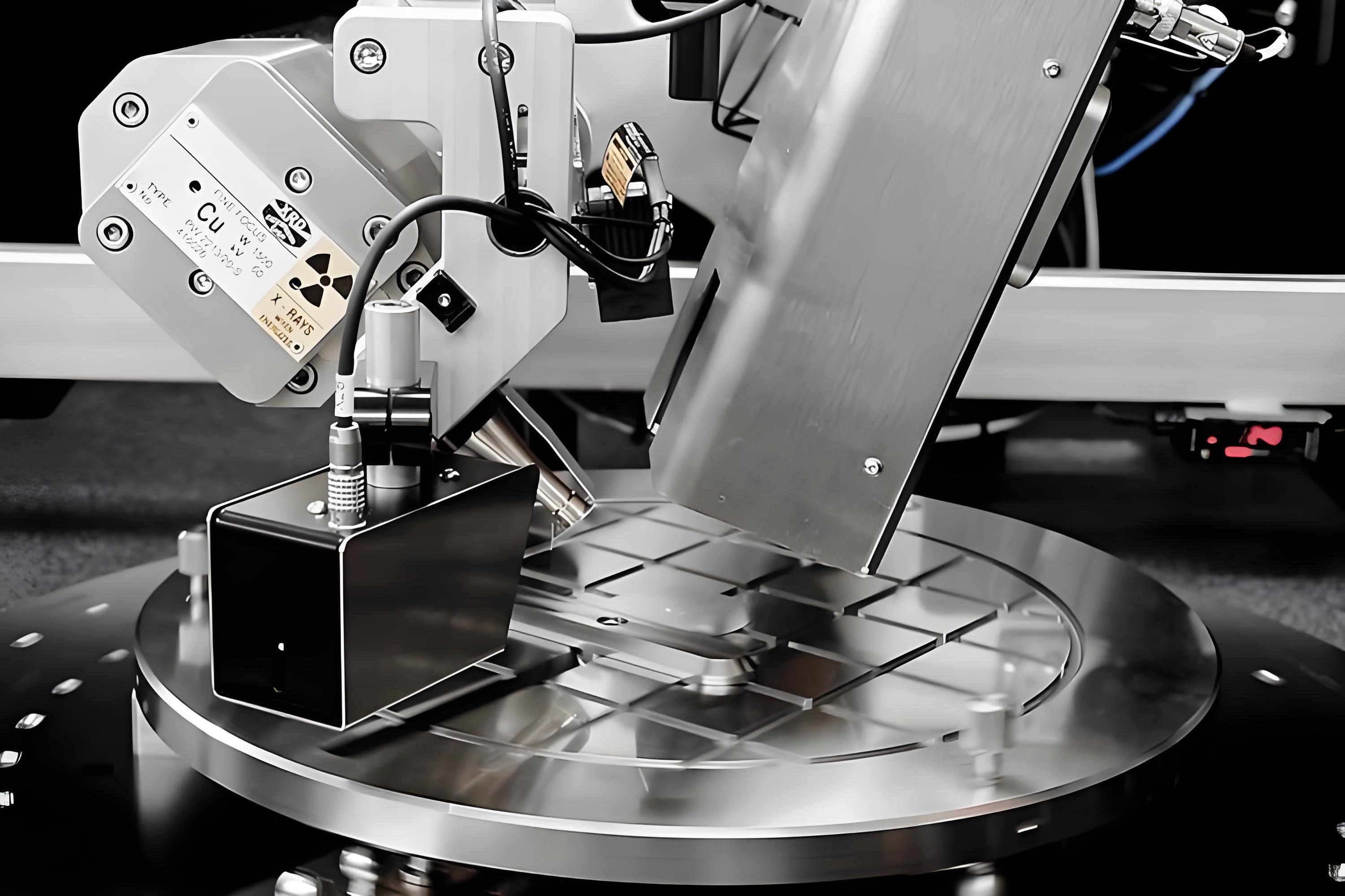
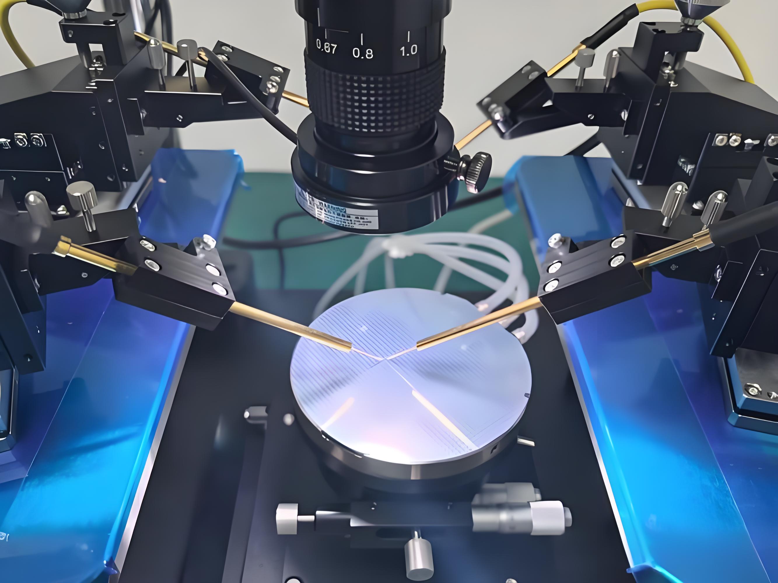
The core advantage of this product is its fully automatic detection capability and ultra-high measurement accuracy, which can meet the strict quality inspection requirements of the semiconductor industry. The granite and stainless steel host has good stability and is not easy to deform, ensuring long-term measurement accuracy. It supports the detection of 200mm and 300mm wafers, and the built-in wafer level metrology analysis software can automatically count the number of defective wafers and generate professional quality reports. The industrial Ethernet interface can be connected to the semiconductor production line control system to realize closed-loop control of production.

https://globalsyt.oss-accelerate.aliyuncs.com/materials/192/0/20260314103435_69b4c93b83541.jpeg

Product specifications:

The main machine dimensions are 2500mm × 2000mm × 1800mm, with a net weight of 1200kg, which is suitable for fixed installation in the semiconductor clean workshop. It supports the detection of 200mm and 300mm wafers, and the measurement accuracy reaches ±0.05μm, meeting the strict quality inspection requirements of the semiconductor industry. The scanning speed is up to 20mm/s, and the fully automatic operation mode can realize unattended detection. It is powered by AC 380V 50/60Hz, and is compatible with major semiconductor production equipment control systems through industrial Ethernet interfaces. The built-in analysis software can generate professional wafer quality inspection reports and conduct data comparison with the design drawings.

https://globalsyt.oss-accelerate.aliyuncs.com/materials/192/0/20260314103346_69b4c90a6739e.jpeg

Product application:

This product is mainly used in wafer manufacturing plants, microelectronic component production workshops, semiconductor packaging and testing plants and other scenarios. It can conduct fully automatic detection of the contour, flatness, step height and other parameters of semiconductor wafers, replace manual detection work, improve detection efficiency and accuracy, and ensure that the delivered semiconductor products meet the design requirements. It can also be used for quality inspection of microelectronic components such as chips and circuit boards.

Frequently Asked Questions (FAQ)

Q:Why is an Automated Wafer Level Profile Metrology System critical for semiconductor fabs?
A:It ensures sub-nanometer thickness uniformity detection, processes 300mm wafers in <60 seconds, and integrates with cleanroom automation - vital for yield management in 5nm/3nm chip production.

Company Profile

Business Type:
Manufacturer
Main Products:
High temperature electric furnace,test chamber,,
Year of Establishment:
2019
Number of Employees:
Address:
Room 712-713, 7th Floor, Building B, No. 91 Hanjiang West Road, Xinbei District, Changzhou City, Changzhou, Jiangsu, China
Average Response Time:
Days

General Information

Business Type:
Manufacturer
Main Products:
High temperature electric furnace,test chamber,,
Year of Establishment:
2019
Number of Employees:
Management System Certification:
HACCP,QS9000,ISO9001,ISO17799,ISO16949,TS16969
Address:
Room 712-713, 7th Floor, Building B, No. 91 Hanjiang West Road, Xinbei District, Changzhou City, Changzhou, Jiangsu, China

Trade Capability

Main Markets:
北美,东欧,大洋洲,西欧,北欧
Shipping Ports:
Export Volume:
Average Lead Time:
Days
Payment Terms:
T/T L/C MoneyGram PayPal D/P Western Union Others
Cooperation Mode:
OEM ODM
Customization Supported:
Yes
Number of Foreign Trade Sales Staff:
Overseas Agent / Overseas Branch:
No

Company Show

Contact this supplier now
*From:
*To:
Mr. Yin Weiwei
Manager / Sales Department
*Message:
Send
New Products
Product Groups
Find Similar Products By Category
scroll_to_top