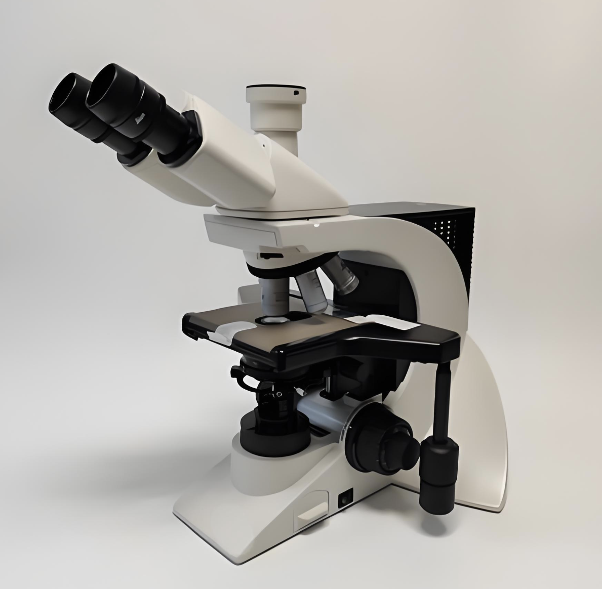


Compared with traditional metallurgical microscopes, this fluorescent model solves the pain point that a single observation mode cannot meet the analysis of composite samples, integrating brightfield observation and multi-channel fluorescent imaging functions, and can switch observation modes with one click. It is equipped with 5 pieces of high-end plan apochromatic objectives, including a 100X oil immersion lens, providing high-resolution imaging effects. It is equipped with a three-channel fluorescent LED light source, supporting three fluorescence excitation modes of UV, blue and green, adapting to common fluorescent staining agents such as DAPI, FITC and TRITC, without manually replacing filter slices and improving detection efficiency. The built-in 8MP high-definition color camera supports synchronous storage and analysis of fluorescent and brightfield images, and can generate composite detection reports.
The maximum magnification is 1600X, equipped with 5 pieces of plan apochromatic objectives (5X/10X/20X/50X/100X oil immersion lens), and comes standard with 10X and 16X wide-field eyepieces, with field of view of 20mm and 12.5mm respectively. The large mechanical sample stage has a size of 240*180mm, supporting X/Y axis stroke of 100*80mm, with a sample clamp fixing device. It is equipped with a three-channel fluorescent LED light source with wavelengths of 365nm (UV), 470nm (Blue) and 550nm (Green), matching standard filter sets. The built-in 8MP CMOS color camera supports 1080P high-definition imaging, and comes with professional image analysis software, which can realize synchronous analysis of metallographic structure and fluorescent markers. The overall size is 500mm*450mm*650mm, with a net weight of 22kg, and the power supply supports 100-240V AC wide voltage adaptation.
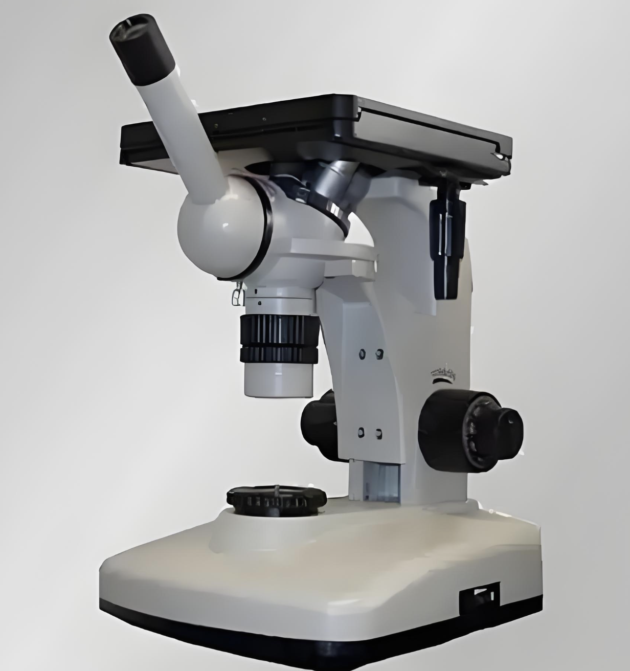
It is mainly used in cross-field scenarios such as semiconductor material defect detection, biological material metallographic analysis, coating material interface observation and medical pathological sample metallographic detection. Typical usage scenarios include: semiconductor wafer defect fluorescent marker detection, composite sample analysis of biological tissue and metal, coating material interface morphology observation, medical metal implant metallographic and fluorescent staining detection, and composite analysis research of new functional materials.


 Post RFQ


 Chat
Chat


 ALL CATEGORIES