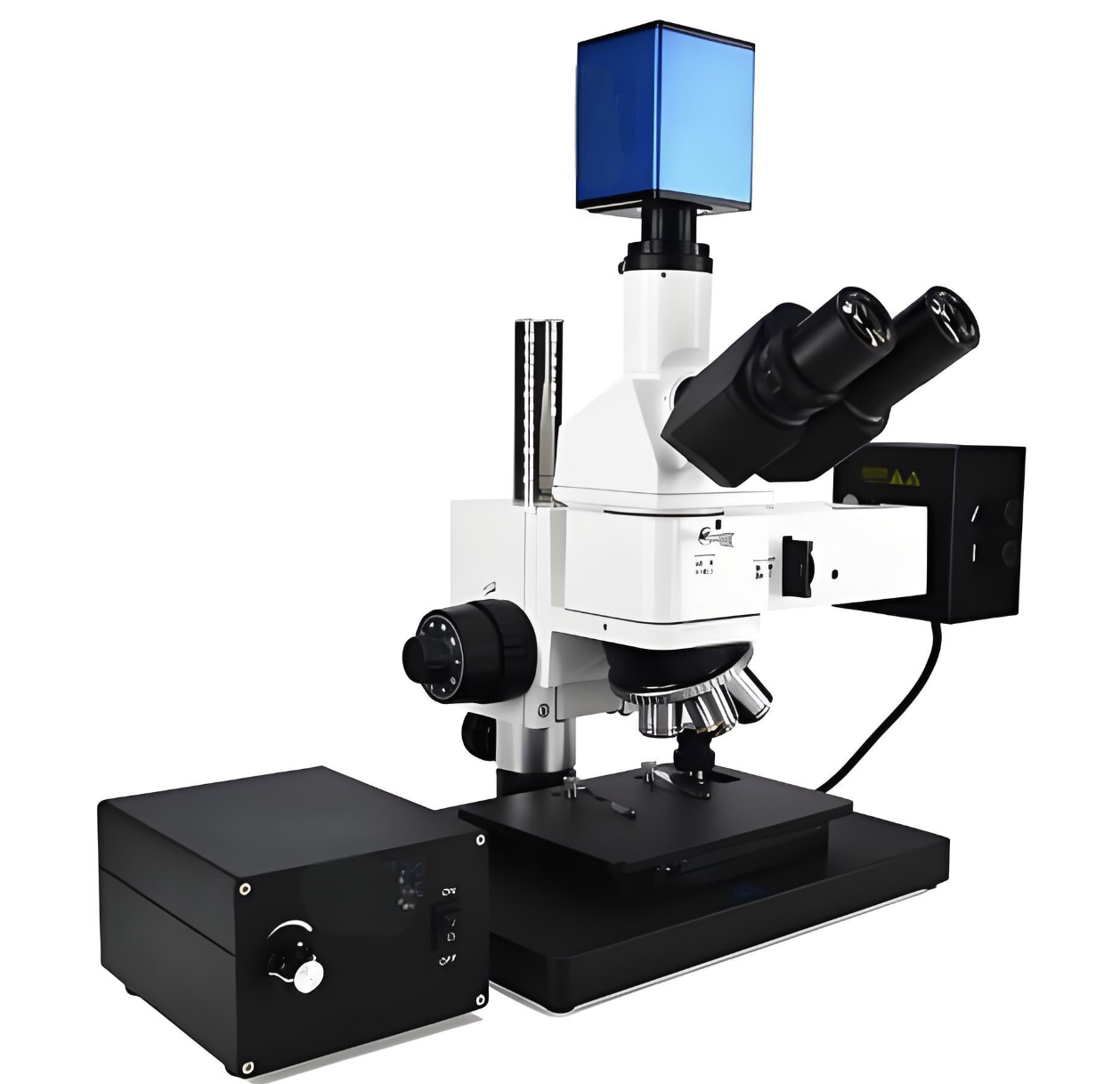


Its core technical highlights include the laser confocal scanning system, which can effectively reduce out-of-focus stray light and obtain high-definition 3D imaging. The dual laser light source is suitable for the observation needs of different types of samples, and the 3D reconstruction software can automatically generate 3D models of surface morphology and roughness detection reports. The imaging accuracy of ≤0.01μm is significantly higher than that of traditional optical microscopes, and it supports automatic scanning of batch samples. Compared with traditional 2D metallurgical microscopes, it can provide more comprehensive microstructure information, supporting the needs of high-end research and high-precision failure analysis.
Overall Dimensions: 850x720x1200mm, Scanning Speed: Max 30 Frames/Second, 3D Imaging Field of View Range: Max 1000x1000μm, Surface Roughness Detection Range: Ra 0.01μm - 100μm, Objective Working Distance: Max 10mm, Host Net Weight: 32.5kg, Package Net Weight: 48kg, Working Environment Temperature: 18-25℃, Relative Humidity: 30-60% without condensation, Compatible with Professional Data Analysis Software.
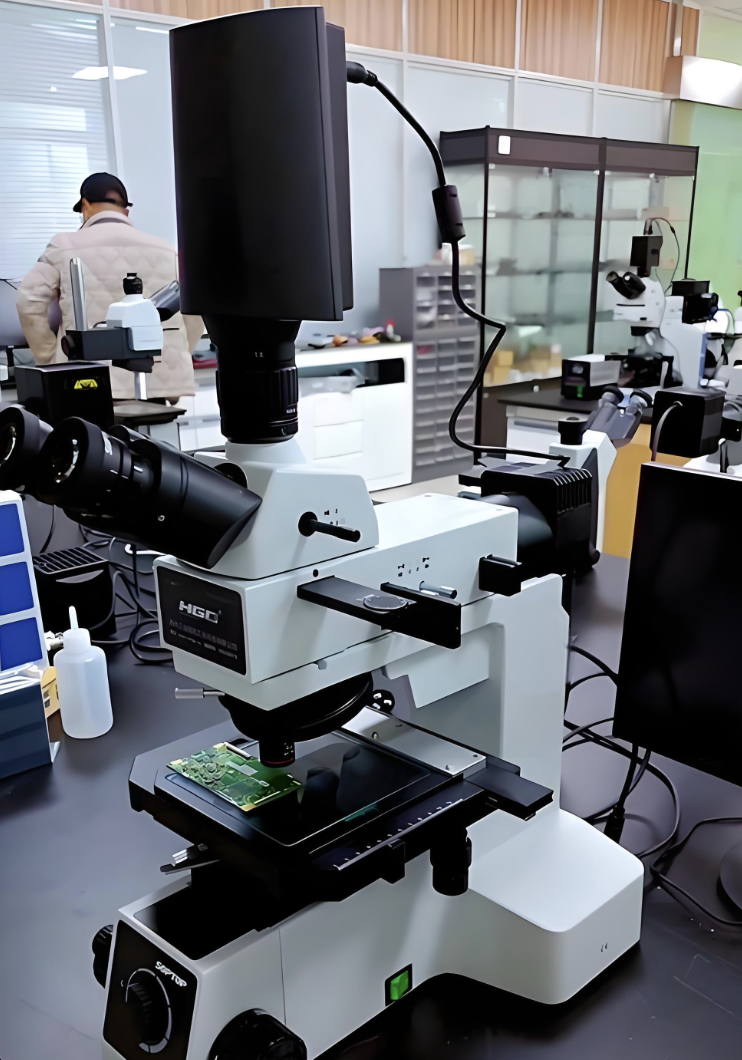
This product is mainly used for failure analysis of semiconductor chip packaging, 3D morphology research of high-end aerospace materials, surface roughness detection of automotive coatings, and microstructure analysis of medical device parts. It is suitable for leading scientific research institutes, semiconductor manufacturing enterprises and third-party leading testing institutions, and can meet the needs of high-precision 3D microstructure observation and quantitative analysis.


 Post RFQ


 Chat
Chat


 ALL CATEGORIES