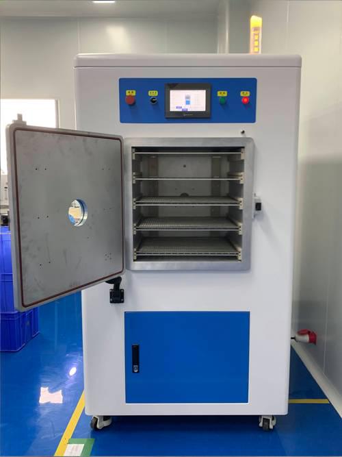
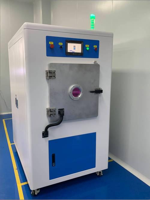


It uses low-temperature plasma technology, ionizing argon and oxygen mixed gas in a vacuum environment to produce plasma. The plasma can undergo chemical reactions with pollutants on the workpiece surface, decomposing them into gases to be discharged, and can form active groups on the workpiece surface to improve surface adhesion and wettability. It is equipped with an industrial-grade PLC touch control system that can customize parameters such as plasma power, gas flow and cleaning time, and automatically complete the whole process of vacuum pumping, plasma cleaning and exhaust. The equipment is equipped with a fully automatic gas control system and vacuum monitoring system, which can monitor the vacuum degree and gas flow in real time to ensure stable and consistent cleaning effects. It also has safety functions such as over-temperature protection and air leakage alarm.
The overall size of the equipment is 180x150x200 Centimeters, and the internal size of the cleaning chamber is 50x50x30 Centimeters, with a maximum load capacity of 100 Kilograms. The working voltage is 380V 50Hz three-phase AC power, with a total power of 10000 Watts, the vacuum degree can reach 10^-3 Torr, the plasma power can be adjusted from 1000 to 5000 Watts, and the gas flow can be adjusted from 10 to 100 SCCM. The net weight of the equipment is 450 Kilograms, and the gross weight is 550 Kilograms. It is equipped with high-precision vacuum sensors and gas flow meters that can accurately control cleaning parameters. The body is made of 304 stainless steel, meeting CE and ISO14001 environmental protection certification standards, and is equipped with a remote monitoring interface to realize remote management and fault diagnosis of the equipment.
It is mainly suitable for semiconductor packaging, multilayer PCB board manufacturing, LED chip packaging, pre-treatment of precision medical device bonding and other scenarios, and can clean semiconductor wafers, inner layers of PCB boards, LED chips, precision medical device components and other workpieces. Typical application scenarios include wafer surface cleaning before semiconductor packaging, adhesion improvement before PCB board lamination, and surface modification before LED chip packaging, which can effectively improve the bonding strength and packaging yield of products, meeting high-precision industrial production requirements.


 Post RFQ


 Chat
Chat


 ALL CATEGORIES