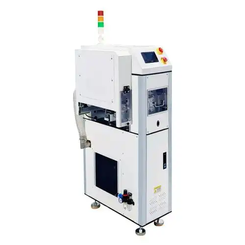
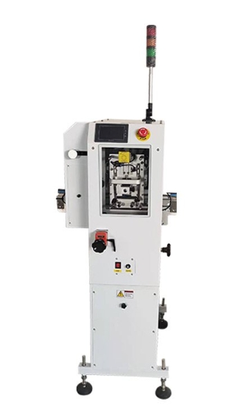


This product adopts vacuum negative pressure assisted ultrasonic cleaning technology combined with constant temperature heating function, allowing the cleaning medium to boil and penetrate into gaps in a vacuum environment, thoroughly removing residues in PCB board via holes and solder joint gaps that are difficult to reach by traditional cleaning. It is equipped with an intelligent touch panel that can customize cleaning time, temperature and vacuum parameters, adapting to cleaning needs of different types of PCB boards. The closed cleaning cavity design avoids environmental pollution caused by volatilization of cleaning medium, and is equipped with a filtration and recovery system that can recycle cleaning solution to reduce usage costs. In addition, the whole machine has a compact size suitable for desktop placement, no need for additional large pipeline installation, and is plug and play.
The overall size of the equipment is 45x35x50 Centimeters, and the internal size of the cleaning chamber is 30x20x10 Centimeters, with a maximum load capacity of 5 Kilograms. The working voltage supports 110V/220V 50/60Hz AC power, with a total power of 800 Watts, the vacuum degree can be adjusted from 5 to 50 Torr, and the maximum heating temperature is 80°C. The net weight of the equipment is 25 Kilograms, and the gross weight is 30 Kilograms. It is equipped with a quick-connector drainage system and a waste liquid recovery box, supporting automatic slag discharge function. The body is made of food-grade 304 stainless steel, corrosion-resistant and easy to clean, meeting EU CE and US FCC safety certification standards.
It is mainly suitable for small PCB processing plants, electronic laboratories, university electronic engineering training centers, smart home accessory manufacturers and other scenarios, and can clean single/multilayer PCB boards, small capacitors and resistors, LED beads, wiring terminals and other precision electronic components. Typical application scenarios include cleaning of solder flux residues after PCB board welding, deep cleaning before electronic component packaging, and component cleaning after maintenance of small electronic equipment, which can effectively improve the welding yield and product service life of electronic components.


 Post RFQ


 Chat
Chat


 ALL CATEGORIES