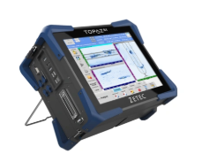
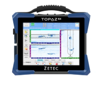


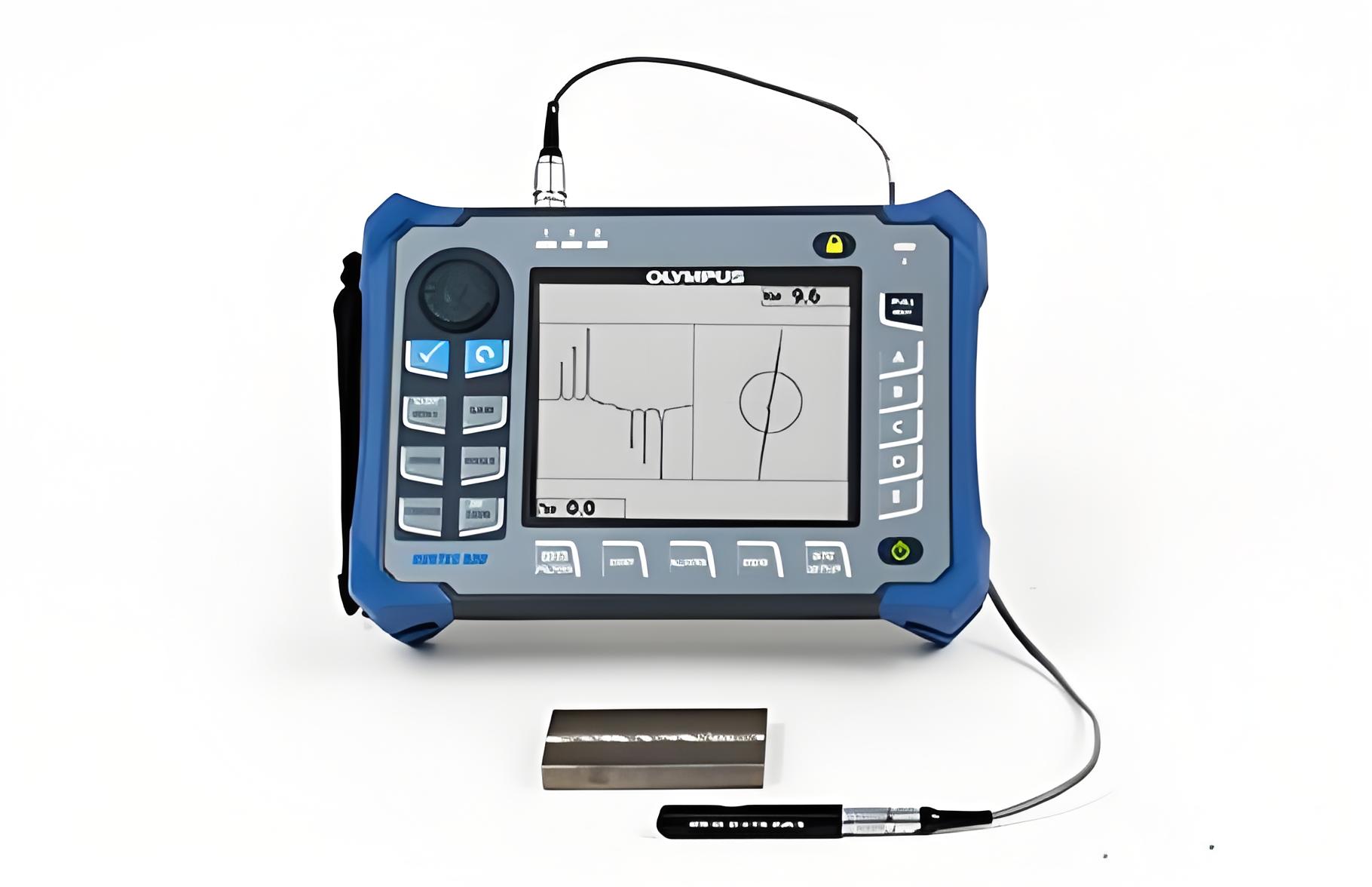
The device adopts high-precision eddy current detection chip and multi-channel signal processing technology, which can identify subtle defects of 0.05mm. Compared with ordinary desktop equipment, the frequency range is expanded to 1Hz~20MHz, adapting to the testing needs of almost all metal materials. It is equipped with a 21.5-inch 1080P high-definition display, which supports multi-window synchronous display of detection waveforms, defect positions and data analysis results, and can manually adjust detection parameters to optimize the detection effect. It supports external connection of multiple types of probes, including array probes and differential probes, which can detect multiple areas at the same time, greatly improving the efficiency of batch detection. The device has built-in professional defect analysis software, which can automatically generate detailed detection reports, and can be connected to the laboratory management system through the Ethernet interface to realize unified data management. It also has electromagnetic shielding design, which can operate stably in complex electromagnetic environments and avoid external interference affecting the detection accuracy.
The overall size of the device is 450mm*320mm*180mm, and it uses AC 100-240V wide voltage power supply, adapting to power standards around the world. It is equipped with array probe interface, which can connect 4 detection probes at the same time to realize multi-area synchronous detection. It supports wide frequency adjustment from 1Hz to 20MHz, and can adjust detection parameters according to the material and thickness of the workpiece to accurately identify different types of defects. It is equipped with USB 3.0, Ethernet and RS232 multiple data interfaces, which can quickly export detection data and connect to external devices. The device shell is made of cold-rolled steel plate spraying process, with good heat dissipation performance and anti-interference ability. It has a built-in cooling fan to ensure stable operation for a long time, and supports wall-mounted installation to save laboratory space.
It is mainly applicable to the defect detection of wafers and lead frames in the semiconductor industry, the solder joint and pin defect detection of precision electronic components, the detection of precision alloy parts in the aerospace field, the quality control of metal parts in medical devices, and the material performance analysis of scientific research institutions. It can complete high-precision and high-frequency detection work in the laboratory environment, meet strict quality standards, and help enterprises improve product pass rate and reduce after-sales costs.


 Post RFQ


 Chat
Chat


 ALL CATEGORIES