Industrial Laser Scanning Microscope
next
prev
Video
1/2

Industrial Laser Scanning Microscope

Price
MOQ
$18999
1 Pieces
Product Details
Scanning Range:
100mm x 100mm
Magnification Range:
20x - 2000x
Laser Type:
635nm Red Visible Laser
Shipping & Policy
Shipping & Delivery Info:
Contact the supplier for details on freight charges and estimated delivery time—tailored to your order and shipping requirements.
Payment Methods:
T/T PayPal
Support payments in USD
Transaction Security Guarantee:
Our platform strictly verifies suppliers’ and buyers’ qualifications to ensure authenticity & legitimacy, creating a reliable trade environment and reducing risks.
After-Sales Support:
For issues like mismatched product quality or delivery delays, we offer assistance—intervening to coordinate and resolve problems per contracts/rules, safeguarding your rights.
Our Store's Similar Products
Product Description
Company Info

Basic Info

This industrial laser scanning microscope is designed for high-precision quality control in manufacturing industries, targeting semiconductor packaging, PCB board production, and precision mechanical parts processing. It solves the pain points of traditional optical microscopes that lack fast 3D scanning capabilities and cannot achieve automated defect detection, enabling efficient, accurate identification of micro-scale defects and dimensional measurements. Equipped with a high-speed laser scanning system, it can quickly generate 3D models of samples and automatically identify common production defects, improving production efficiency and reducing manual inspection errors.

Key attributes

Scanning Range
100mm x 100mm
Magnification Range
20x - 2000x
Laser Type
635nm Red Visible Laser
Detection Accuracy
0.1μm
Scanning Speed
30 FPS
Software
3D Reconstruction & Defect Inspection Suite
Interface Types
Gigabit Ethernet, USB 3.0
Power Supply
110/220V AC
Sample Stage Load Capacity
5kg
Working Environment
20-25℃, 40-60% Humidity
Body Dimensions
450mm(W) x 600mm(D) x 350mm(H)

Customer reviews

John Carter · Research Scientist
The Industrial Laser Scanning Microscope has been a game-changer for our materials research. The high-resolution imaging capabilities allow us to analyze surface structures with incredible precision. We've used it extensively for quality control in our semiconductor manufacturing process, and it has significantly reduced our defect rates. The automated scanning feature saves us hours of manual work.

Product Description

Product features:

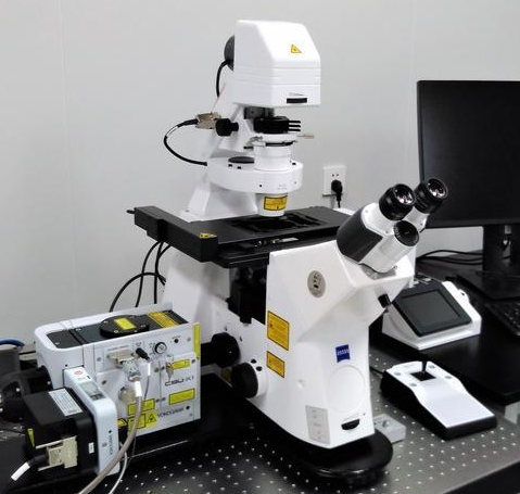
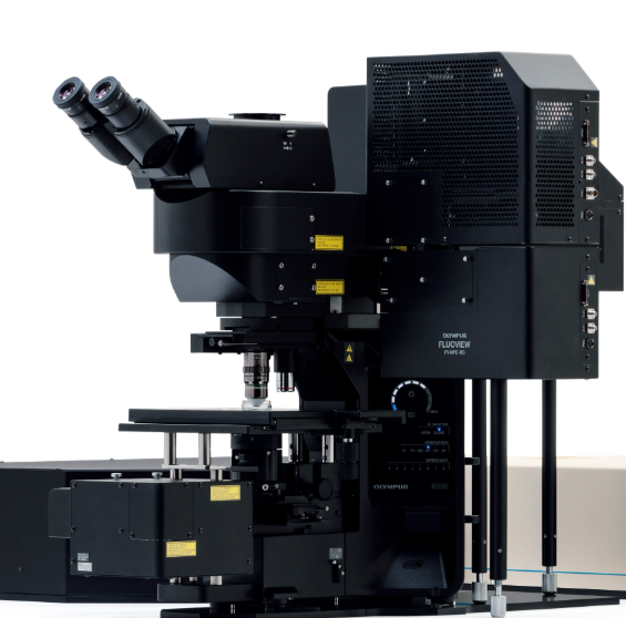
The key advantages of this industrial laser scanning microscope include its large scanning range of 100mm x 100mm, high detection accuracy of 0.1μm, and fast scanning speed of 30 frames per second, allowing rapid inspection of large samples. The dedicated 3D reconstruction and defect inspection software can automatically identify common defects such as solder ball abnormalities, circuit short circuits, and surface scratches, and generate detailed inspection reports. It supports batch sample inspection and can export data in CAD format for integration with existing production quality management systems. The high-precision electric sample stage ensures stable and accurate positioning of samples, reducing the need for manual adjustment and improving inspection consistency.

https://globalsyt.oss-accelerate.aliyuncs.com/materials/205/0/20260311103853_69b0d5bd72831.PNG

Product specifications:

The industrial laser scanning microscope has a scanning range of 100mm x 100mm, with a maximum magnification range of 20x to 2000x and a transverse detection accuracy of 0.1μm. It is equipped with a 635nm red visible laser that can be adjusted for focal length, and a high-precision electric sample stage with a load capacity of up to 5kg. The device is powered by 110/220V AC, with overall dimensions of 450mm (W) x 600mm (D) x 350mm (H). It supports Gigabit Ethernet and USB 3.0 data transmission, enabling fast transfer of large-volume inspection data. The working environment requires a temperature of 20-25℃ and relative humidity of 40-60% to ensure stable operation and imaging quality.

Product application:

This industrial laser scanning microscope is widely used in semiconductor packaging solder joint defect detection, PCB circuit board micro-short circuit detection, precision hardware parts surface roughness analysis, medical device parts micro-crack detection, and aerospace precision component micro-dimensional measurement. It can help manufacturing enterprises improve product quality, reduce scrap rates, and meet the high-precision testing requirements of modern industrial production.

Frequently Asked Questions (FAQ)

Q:What are the key features of an Industrial Laser Scanning Microscope?
A:Industrial Laser Scanning Microscopes offer high-speed imaging (up to 30fps), sub-micron resolution (0.1μm), and multi-layer scanning. Key applications include semiconductor inspection and precision component measurement, with laser wavelengths typically ranging from 405nm to 785nm.

Company Profile

Business Type:
Manufacturer
Main Products:
Instrumentation,electromechanical equipment,electronic components,
Year of Establishment:
2011
Number of Employees:
Address:
Room 3, No. 658 Xinzhen Road, Zhoushi Town, Kunshan City, Suzhou, Jiangsu, China
Average Response Time:
Days

General Information

Business Type:
Manufacturer
Main Products:
Instrumentation,electromechanical equipment,electronic components,
Year of Establishment:
2011
Number of Employees:
Management System Certification:
HACCP,TL900,QS9000,SA8000,ISO9001,ISO9004,ISO17799,ISO9000,ISO14000,ISO10441,ISO16949,TS16969,ISO19011:2000,OHSAS18001,Others
Address:
Room 3, No. 658 Xinzhen Road, Zhoushi Town, Kunshan City, Suzhou, Jiangsu, China

Trade Capability

Main Markets:
北美,南美洲,东欧,东南亚,非洲,大洋洲,中东,东亚,西欧,中美洲,北欧,南欧,南亚,国内市场
Shipping Ports:
Export Volume:
Average Lead Time:
Days
Payment Terms:
T/T L/C MoneyGram PayPal D/P Western Union Others
Cooperation Mode:
OEM
Customization Supported:
Yes
Number of Foreign Trade Sales Staff:
Overseas Agent / Overseas Branch:
No

Company Show

Contact this supplier now
*From:
*To:
Mr. Yang Lei
manager /
*Message:
Send
New Products
Product Groups
Find Similar Products By Category
scroll_to_top