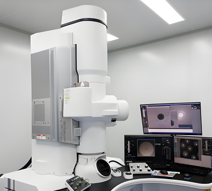
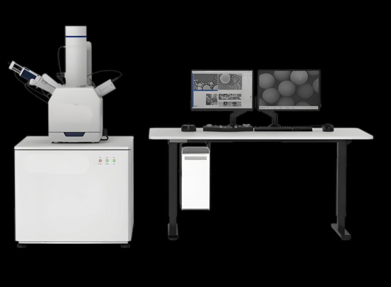


The core advantages of this automated laser microscope lie in its fully automated detection workflow, which can complete sample placement, focusing, imaging and defect analysis autonomously without manual intervention. It adopts a high-power visible laser scanning system, which can clearly detect micro-defects as small as 0.1μm on metal, plastic and semiconductor surfaces. The built-in AI defect recognition algorithm can automatically classify and quantify defects, greatly improving the efficiency of quality control. It also supports remote monitoring and data uploading through the industrial Ethernet interface, meeting the requirements of intelligent factory data interconnection.
The main specifications include: overall dimensions of 1200mm (length) × 800mm (width) × 1500mm (height), net weight of 350kg, power input of 220VAC 50Hz, maximum power consumption of 1800W. The automated stage supports X/Y/Z axis precise movement, with a maximum travel of 100mm×100mm×50mm. It is equipped with a 6-position automatic lens turret, supporting objective lenses ranging from 5x to 50x. The AI analysis software supports custom defect detection templates, and can export standard quality control reports in PDF format.
This product is mainly suitable for industrial precision component inspection scenarios such as semiconductor wafer defect detection, precision hardware size measurement, plastic part surface defect detection and electronic component quality control. It is widely used in semiconductor manufacturing, aerospace parts processing, consumer electronics manufacturing and other industries. For example, semiconductor manufacturers can use it to automatically detect micro-cracks and contaminants on wafer surfaces, achieving 100% full-inspection of mass-produced wafers.


 Post RFQ


 Chat
Chat


 ALL CATEGORIES