Basic Info
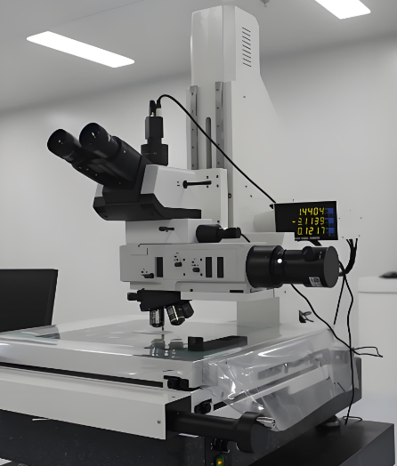
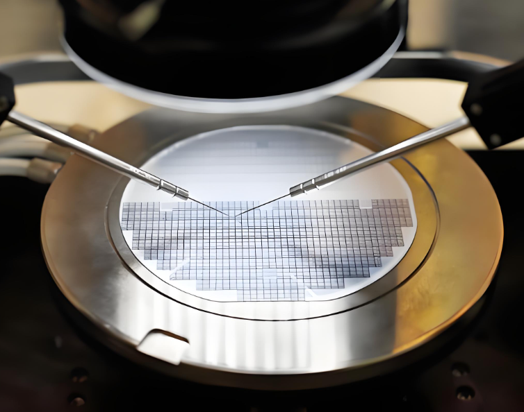
This wafer inspection laser microscope is a high-precision testing device tailored for semiconductor manufacturing and wafer packaging industry. It uses laser confocal imaging technology to achieve sub-micron resolution detection of wafer surface defects, roughness and alignment errors. It supports automatic batch detection of 300mm standard wafers, meeting the high-precision and high-efficiency testing requirements of semiconductor production lines.
Customer reviews

David · Electronics Repair Specialist
The Handheld Laser Digital Microscope has become my most trusted tool for PCB diagnostics. The 500x magnification with laser illumination reveals solder joint cracks and trace defects that are invisible to the naked eye. Its ergonomic design allows comfortable use during extended repair sessions, and the built-in measurement tools provide instant dimensional verification of components.
Product Description
Product features:
The core advantages of this microscope include ultra-high 0.1μm imaging resolution, ±0.05μm stage positioning accuracy, and AI-powered automatic defect identification function. It solves the pain points of traditional wafer inspection equipment having low detection efficiency and high missed detection rate, and the professional semiconductor analysis software can automatically generate defect reports and provide data support for process optimization.
Product specifications:
Key specifications include 50x-2000x magnification range, 532nm green laser source with 0-15mW adjustable power, 100mm²/s scanning speed, and compatible objective lenses of 5x/20x/50x/100x/1000x Oil. The device is equipped with a built-in constant temperature control system to ensure stable performance during long-term testing, and supports connection to industrial production line management systems.
Product application:
This wafer inspection laser microscope is applied in semiconductor wafer defect detection, chip packaging quality inspection, MEMS device surface analysis, and solar cell panel precision testing. It provides professional detection solutions for semiconductor manufacturing plants and electronic component production enterprises.
Frequently Asked Questions (FAQ)
Q:What specifications are critical for a Wafer Inspection Laser Microscope in semiconductor manufacturing?
A:Requires <0.05μm resolution, automated defect classification (ADC), and 300mm wafer compatibility. Key for detecting sub-10nm particles with throughput >60 wafers/hour in cleanroom environments.


 Post RFQ


 Chat
Chat


 ALL CATEGORIES