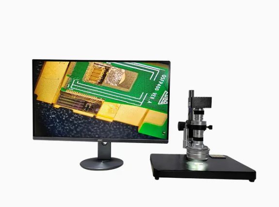
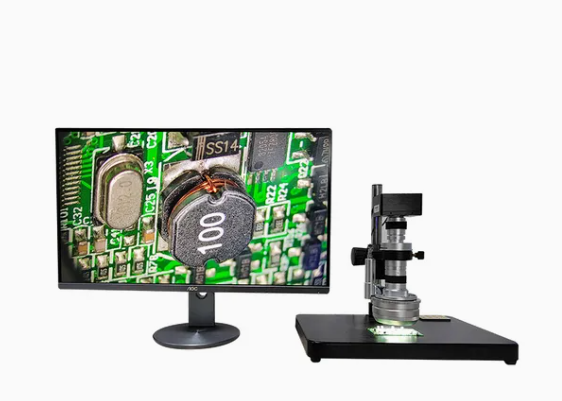


Compared with ordinary commercial 3D microscopes, this product has micron-level 3D reconstruction accuracy, and is equipped with a 7-band multi-spectral lighting system, which can realize spectral imaging of different bands for analyzing the chemical composition and microstructure of materials. The motorized precision stage supports automatic movement of the XYZ three axes, which can realize automatic scanning and 3D model stitching of large-area samples. The 24MP 8K ultra-high-definition camera can output extremely clear microscopic images, and the built-in professional analysis software is compatible with scientific research tools such as CAD and MATLAB, supporting data export and sharing. The aerospace-grade aluminum alloy body ensures long-term stable operation, reducing the impact of vibration on imaging accuracy. It supports UPS backup power supply, solving the problem of data loss caused by power outages in scientific research scenarios, providing a reliable high-precision inspection platform for cutting-edge scientific research.
The body size is 800*600*1000mm, the magnification range is 100-10000X, the 3D reconstruction accuracy can reach ±0.001mm, and it is equipped with a 7-band multi-spectral LED lighting system. The electric stage stroke is X-axis 300mm, Y-axis 200mm and Z-axis 100mm, and it is equipped with a 24MP 8K CMOS camera. It supports USB3.1, HDMI2.1 and Gigabit Ethernet data transmission, and the built-in professional scientific research analysis software is compatible with Windows/Linux operating systems. It uses an aerospace-grade aluminum alloy body, the total weight is about 80kg, the working temperature range is 18-28℃, the working humidity is 20%-60%RH, the power supply is AC 110/220V 50/60Hz and supports UPS backup power supply, and it has passed ISO17025 laboratory certification and CE, FCC safety certifications.
It is mainly used for nanomaterial microstructure analysis, precision mechanical parts size measurement, biological molecular structure research, semiconductor chip defect detection and aerospace material performance testing. University scientific research teams can carry out cutting-edge material research through this equipment, and semiconductor manufacturing enterprises can detect nano-level defects on the chip surface, improving the quality control level of chip production, providing strong technical support for the research and development and quality inspection of high-end manufacturing industries.


 Post RFQ


 Chat
Chat


 ALL CATEGORIES