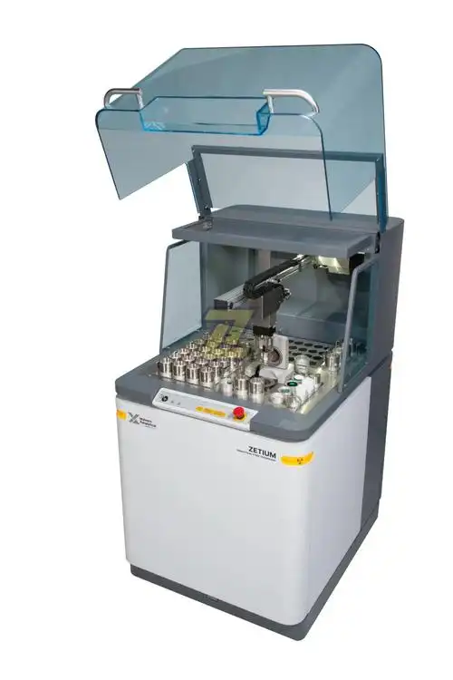
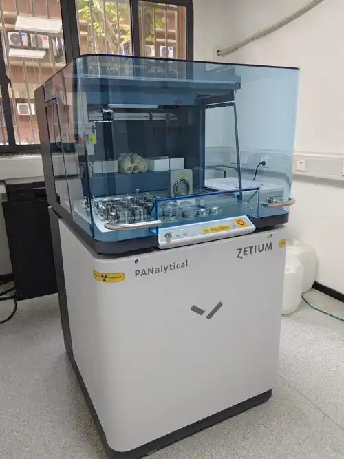


The core advantage of this micro-XRF spectrometer is its ultra-high spatial resolution, which can achieve element analysis of samples with a minimum size of 1μm thickness × 10μm diameter. It adopts a cooled silicon drift detector, ensuring high spectral resolution and low background noise, improving the detection sensitivity of trace elements. The built-up optical microscope with up to 1000× magnification allows users to quickly locate the detection area, improving the accuracy of sample detection. The 3D element distribution mapping software can visually display the element distribution of the sample, helping users deeply analyze the microstructure and component distribution of the sample. Compared with traditional XRF equipment, it has a high-precision sample stage, which can achieve precise movement of the sample in three directions, meeting the needs of multi-point detection and area scanning.
The overall dimensions of the instrument are 1200mm × 800mm × 1500mm, with a total weight of 800kg. It is equipped with a high-precision motor-driven sample stage, with a movement range of X:100mm, Y:100mm and Z:50mm, and the positioning accuracy is ≤1μm. The excitation voltage is adjustable from 0-50kV, and the excitation current is adjustable from 0-100μA. The spatial resolution is ≤5μm, and the spectral resolution is ≤130eV at Mn Kα, covering all elements from sodium to uranium. The 3D element distribution mapping software can generate 2D and 3D element distribution images, and support data export in multiple formats.
This micro-XRF spectrometer is mainly applicable to cultural relics protection and archaeological research, such as non-destructive analysis of ancient ceramics, bronze wares, calligraphy and painting pigments, providing scientific basis for cultural relics restoration and age identification. It is also suitable for micro-material analysis in the semiconductor industry, such as detecting the element distribution of micro-chips, solder joints and other micro-components, and analyzing the quality of micro-electronic devices. In addition, it can be used for forensic trace evidence analysis, such as detecting the element components of trace paint, fiber and other evidence, providing scientific support for criminal investigation.


 Post RFQ


 Chat
Chat


 ALL CATEGORIES